high-performance and flexible ZnO TFTs
The micro-nanoelectronic device research group has made important progress in the field of high-performance and flexible ZnO TFTs
In the past two years, IEEE Electron Device Letters has published the research results of high-performance and flexible Zinc oxide (ZnO) thin-film transistors (TFTs) by Professor Yanqing Wu. The papers entitled “High-Performance Flexible ZnO Thin-Film Transistors by Atomic Layer Deposition” and “Performance Optimization of Atomic Layer Deposited ZnO Thin-film Transistors by Vacuum Annealing”. The first author of this paper is Mengfei Wang, a PhD student of Grade 2016 from school of optical and electronic information, Huazhong University of Science and Technology. The other authors from group members including Xuefei Li, Xiong Xiong, Shengman Li, Qianlan Hu, Jian Song, Xin Wang, Dan Zhan, and Chengru Gu.
As a widely studied oxide semiconductor, ZnO has the advantages of wide band gap, transparency, high mobility and low production cost. Based on the advantage that large area thin films could be deposited at a low temperature using ALD technique, different from the previous magnetron sputtering technique, ALD was used to prepare ZnO TFTs at 190°C. It is essential to optimize the electrical performance in both on-state and off-state of the ALD ZnO thin-film transistors. However, it’s difficult to achieve this requirement by annealing under hydrogen, oxygen, nitrogen, or atmospheric atmospheres. In response to this problem, ALD ZnO TFTs were annealed in vacuum at different temperatures to optimize the electrical performance.
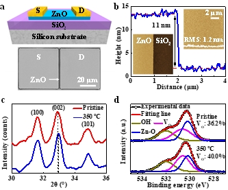
Fig. 1. (a) Top: Cross-section schematic view of the ZnO TFT, bottom: SEM image. Scale bar: 20 µm. (b) AFM images of the device. Scale bar: 2 µm. (c) XRD spectra of pristine and 350 ℃-annealed ZnO films. (d) XPS spectra of pristine and 350 ◦C-annealed ZnO films in the O 1s region.
The field-effect mobility (μFE) was improved from 18.5 cm2/V·s to a record high 43.2 cm2/V·s while maintaining a large Ion/Ioff ratio of 5×10⁹ after rapid thermal annealing (RTA) under vacuum at 350 ℃. The mechanism of significant performance improvement was investigated in details by XRD, XPS, and 1/f noise measurement. The excellent performance can be attributed to the improvement in the ZnO channel and the interface. The oxygen vacancy ratio in ZnO increases from 36.2% to 40.0%. The interface trap density (Nit) between silicon oxide (SiO2) and ZnO decreases from 5.1×10¹¹ eV-1cm-2 to 1.4×10¹¹ eV-1cm-2. Furthermore, the oxide trap density (Not) of the SiO2 dielectric reduces from 3.7×10¹⁹ eV-1cm-3 to 1.1×10¹⁹ eV-1cm-3. Electrical characteristics of the 350 ℃-annealed device at different measurement temperatures varying from 20 to 180 ℃ have been analyzed. The results of our work show that the electrical performance of ZnO TFTs can be greatly improved by vacuum annealing and can be further optimized with a high-κ dielectric for high-performance display or logic applications.
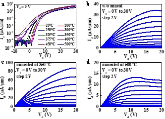
Fig. 2. (a) Transfer characteristics as a function of annealing temperature from 20 to 500 ℃. Output characteristics for the device annealed at (b) 20 ℃, (c) 350 ℃, and (d) 500 ℃, respectively.
In the second work, the application research of zinc oxide thin film transistors in the flexible field is becoming more and more popular. Mobility and bending stability are the key metrics for flexible electronics. However, flexible ZnO TFTs prepared by pulsed laser deposition, magnetron sputtering, solution method, or printing method are difficult to achieve high mobility and high bending stability at the same time. In response to this problem, our team continued to fabricated flexible ZnO TFTs use ALD technique.
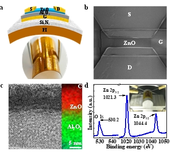
Fig. 3. (a) Top: schematic of the flexible ZnO TFT, bottom: optical image of a flexible sample. (b) SEM image of the device. (c) HRTEM and HAADF images of Al2O3 dielectric and ZnO channel. Scale bar: 5 nm. (d) XPS spectrum in O 1s and Zn 2p regions, the insert is a flexible sample attached to an aluminum cylinder.
Based on the advantages of the ALD technique, our team deposited a large area of uniform and high-quality dielectric and channel materials at a low temperature, and obtained a high-quality material interface. The flexible ZnO TFT has achieved a mobility of 13 cm2/V·s and an Ion/Ioff of 1.5×10⁸. The flexible device also achieves excellent bending stability. The flexible ZnO device exhibits excellent electrical characteristics even after being bent for 200,000 cycles with a tensile strain of 0.63%. Electrical measurement under a high tensile strain of 2.08% has also been carried out. Moreover, the electrical performance dependence of flexible ZnO TFTs with a tensile strain of 0.78% on temperature from 20 ℃ to 140 ℃ has been investigated for the first time. These results indicate the potential of ALD ZnO TFTs for flexible electronic applications.
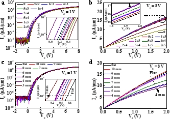
Fig. 4. (a) Transfer characteristics and (b) output characteristics as a function of bending cycle from 0 to 200,000, respectively. Bending radius is fixed at 10 mm. (c) Transfer characteristics and (d) output characteristics as a function of bending radius, respectively.
文章链接:https://ieeexplore.ieee.org/document/8629034
文章链接:https://ieeexplore.ieee.org/abstract/document/9387336